
4EJ524 Analogue and Digital Electronics
Table of Contents
A.) The Current at Collector 5
B.) Emitter-Collector Voltage 5
C.) If transistor is saturated or not ?. 6
D.) Base Resistance value – Driving transistor?. 6
5) Inverting Op Amp circuit 13
Introduction:
Analog and digital circuits are used for transmitting and processing information like sound, light to form a continuous variable signal. Analog is capable of routing the signals directly whereas digital circuitry will change the analogue into regular wave form or pulses, which means there is alteration of signal in digital circuit. This work with examples of various analog and digital circuits will give an knowledge and understanding of analog and digital circuits.
Task
1. Simulating the circuit and calculation of parameters, gain of transistor is 150.
Answer: Bipolar junction transistor has collector as amplifier. The configuration has input voltage applied to base of transistor. The output signal is taken out of emitter of transistor. The collector forms a common path to input and output circuit. The configuration is called common collector. The collector terminal is grounded to earth with support of power supply.
Another type of bipolar junction transistor is named as Base Amplifier. The circuit has a base, common to input and output voltage. This configuration is called as common base (CB). This is not so commonly used amplifier as compared to common collector or common emitter. This has certain unique input and output performance characters as compared to other ones.
In common emitter mode, the input comes from base having collector at output side. The common point to input and output is emitter. This implies the base and emitter is called as input termination. Common emitter terminals are grounded. Hence this configuration is referred to as grounded emitter configuration. This is called as CE configuration. This type of CE transistor is commonly used in electronics. Input is given to base and emitter and output is drawn at collector, emitter being common.
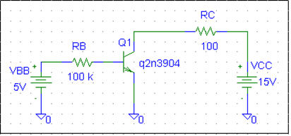
Solution:
In the above, Vcc is the Voltage at the collector, Vbb is the voltage at the base, Rc is the collector resistance and Rb is the base resistance.
The NPN transistor consist two diodes. One portion of the diode is called an emitter to the base and the other portion is called as a collector to base diode. Therefore three terminals namely N, P and N are present. Terminals are the emitter, collector and base. NPN transistors have low doping in the middle and influence working of transistors. Doping is moderate in the emitter and is heavy the collector.
A.) The Collector current
This is alluded to as the current of return of transistor which is found in the gatherer terminal. The present authority and furthermore base current are aftereffects of vitality transmitted through the producer circuit. There is a division at the base